| CPC H01Q 1/38 (2013.01) [G11C 11/16 (2013.01); H01F 10/14 (2013.01); H01F 38/14 (2013.01); H04B 5/26 (2024.01); H01F 2038/143 (2013.01); H04L 27/2636 (2013.01)] | 18 Claims |

|
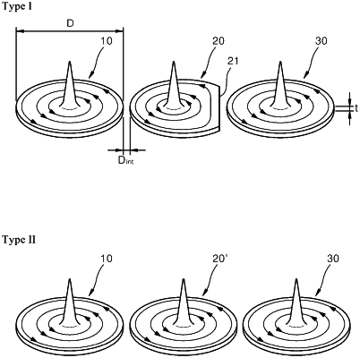
1. A signal transferring device, comprising:
a first structure that includes a first magnetic thin film structure having a first magnetic vortex configured to receive a signal as an input signal;
a second structure that is spaced apart from at least one side of the first structure, the second structure including a second magnetic thin film structure having a second magnetic vortex configured to transfer the signal; and
a third structure that is spaced apart from at least one side of the second structure, the third structure including a third magnetic thin film structure having a third magnetic vortex configured to output the signal from the signal transferring device,
wherein
the first and third structures have a symmetrical shape, and
the second structure has an asymmetrical shape.
|