| CPC H01M 50/507 (2021.01) [H01M 50/50 (2021.01); H01M 50/502 (2021.01); H01M 50/519 (2021.01)] | 9 Claims |

|
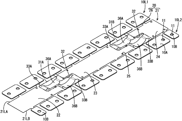
1. A connection module that can be attached to an electricity storage element group composed of a plurality of electricity storage elements each including electrode terminals, and that connects the plurality of electricity storage elements, comprising:
a flexible printed circuit board; and a plurality of connecting members that are connected to the flexible printed circuit board, and that connect the electrode terminals of adjacent electricity storage elements to each other,
wherein the flexible printed circuit board includes a pair of first side edges,
the plurality of connecting members constitute a first connecting member row disposed so as to be arranged along one of the pair of first side edges, and a second connecting member row disposed so as to be arranged along the other of the pair of first side edges,
the flexible printed circuit board includes a tolerance absorbing portion including a slit extending in the same direction as the pair of first side edges, and a pair of deflection portions disposed with the slit interposed therebetween, and is divided into a plurality of connecting member placement portions by the tolerance absorbing portion,
wherein the slit and the pair of deflection portions are formed in a surface of the flexible printed circuit board that is defined between the pair of first side edges,
and
the pair of deflection portions can be deflected in a direction in which the two connecting member placement portions that are adjacent to each other with the tolerance absorbing portion interposed therebetween move toward and away from each other.
|