|
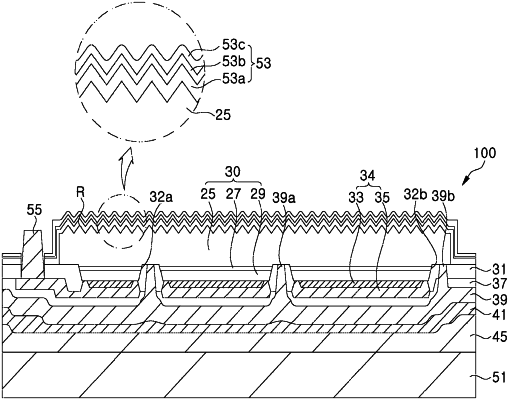
1. A light emitting diode comprising: a support substrate; a first conductivity type semiconductor layer disposed on the support substrate; an upper insulation layer disposed on the first conductivity type semiconductor layer and comprising a plurality of material layers; a mesa comprising an active layer and a second conductivity type semiconductor layer and disposed under a partial region of the first conductivity type semiconductor layer to expose an edge of the first conductivity type semiconductor layer, the mesa having a plurality of first through-holes and a plurality of second through-holes exposing the first conductivity type semiconductor layer through the second conductivity type semiconductor layer and the active layer; a first electrode disposed between the second conductivity type semiconductor layer and the support substrate, the first electrode comprising: first contact portions electrically connected to the first conductivity type semiconductor layer through the plurality of first through-holes; and second contact portions electrically connected to the first conductivity type semiconductor layer through the plurality of second through-holes; a second electrode disposed between the first electrode and the second conductivity type semiconductor layer and electrically connected to the second conductivity type semiconductor layer; and at least one upper electrode pad disposed adjacent to the first conductivity type semiconductor layer and connected to the second electrode; a first insulation layer disposed between the mesa and the support substrate; a second insulation layer interposed between the first electrode and the second electrode; and a reflection layer disposed between the second insulation layer and the first electrode; wherein one or more of the plurality of first through-holes are surrounded by the active layer and the second conductivity type semiconductor layer and are disposed within a region surrounded by edges of the mesa; and one or more of the plurality of second through-holes are partially surrounded by the active layer and the second conductivity type semiconductor layer and are disposed along the edges of the mesa.
|
