|
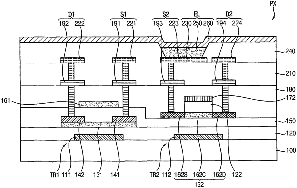
1. A display device, comprising: a first gate electrode disposed on a substrate; a buffer layer disposed on the first gate electrode; a first active pattern disposed on the buffer layer, overlapping the first gate electrode, and including an oxide semiconductor; a source pattern and a drain pattern respectively disposed on ends of the first active pattern; an insulation layer overlapping the source pattern and the drain pattern on the buffer layer; an oxygen supply pattern disposed on the insulation layer, overlapping the first active pattern, and supplying oxygen to the first active pattern; a second active pattern disposed on the insulation layer and completely spaced apart from the oxygen supply pattern in a direction parallel to a main surface of the substrate, the second active pattern including: a channel region; and a source region and a drain region respectively disposed on ends of the channel region; an insulation pattern disposed on the channel region of the second active pattern; and a second gate electrode disposed on the insulation pattern.
|
