| CPC H01L 29/78696 (2013.01) [B82Y 10/00 (2013.01); H01L 27/0207 (2013.01); H01L 27/092 (2013.01); H01L 27/11807 (2013.01); H01L 29/0673 (2013.01); H01L 29/42392 (2013.01); H01L 21/823807 (2013.01); H01L 21/823871 (2013.01); H01L 29/775 (2013.01)] | 20 Claims |
|
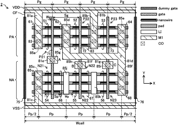
1. A semiconductor integrated circuit device comprising
a first standard cell constituting a NAND gate and including first and second p-type nanowire field effect transistors (FETs), and first and second n-type nanowire FETs,
the first and second p-type nanowire FETs are connected together in parallel, and the first and second n-type nanowire FETs are connected together in series,
each of the first and second p-type nanowire FETs and the first and second n-type nanowire FETs including:
a nanowire extending along a first direction, the nanowire being a single nanowire or including a plurality of nanowires;
first and second pads arranged at both ends of the nanowire in the first direction, and connected to the nanowire; and
a gate electrode extending along a second direction perpendicular to the first direction, and surrounding a periphery of the nanowire, wherein:
the first pad of the first p-type nanowire FET, the first pad of the second p-type nanowire FET, and the second pad of the second p-type nanowire FET are arranged at a first pitch in the first direction,
the first pad of the first n-type nanowire FET, the first pad of the second n-type nanowire FET, and the second pad of the second n-type nanowire FET are arranged at the first pitch in the first direction,
a cell width of the first standard cell that is a dimension of the first standard cell in the first direction is an integral multiplication of the first pitch, and
the gate electrode of the first p-type nanowire FET and the gate electrode of the first n-type nanowire FET are integrally formed with each other as a first gate line extending in the second direction, the gate electrode of the second p-type nanowire FET and the gate electrode of the second n-type nanowire FET are integrally formed with each other as a second gate line extending in the second direction.
|