| CPC H01L 29/7869 (2013.01) [H01L 21/02554 (2013.01); H01L 21/02565 (2013.01); H01L 21/02631 (2013.01); H01L 29/04 (2013.01); H01L 29/045 (2013.01); H01L 29/2206 (2013.01); H01L 29/221 (2013.01); H01L 29/24 (2013.01); H01L 29/263 (2013.01); H01L 29/42356 (2013.01); H01L 29/45 (2013.01); H01L 29/4908 (2013.01); H01L 29/66969 (2013.01); H01L 29/78693 (2013.01); H01L 29/78696 (2013.01)] | 5 Claims |
|
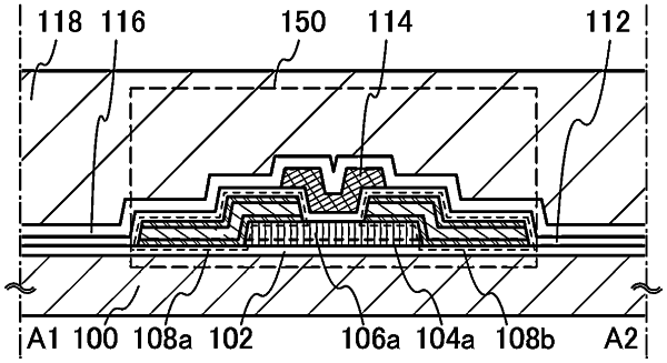
1. A semiconductor device comprising:
a first transistor comprising silicon in a channel formation region; and
a second transistor comprising an oxide semiconductor in a channel formation region,
wherein a first insulating layer is provided over the channel formation region of the first transistor,
wherein a first gate electrode of the first transistor is provided over the first insulating layer,
wherein a second insulating layer is provided over the first gate electrode of the first transistor,
wherein a layer comprising the channel formation region of the second transistor is provided over the second insulating layer,
wherein a third insulating layer is provided over the layer comprising the channel formation region of the second transistor,
wherein a second gate electrode of the second transistor is provided over the third insulating layer,
wherein a fourth insulating layer is provided over the second gate electrode of the second transistor,
wherein a fifth insulating layer is provided over the fourth insulating layer,
wherein one of a source electrode and a drain electrode of the first transistor is electrically connected to one of a source electrode and a drain electrode of the second transistor via an opening provided in the second insulating layer, an opening provided in the third insulating layer, an opening provided in the fourth insulating layer, and an opening provided in the fifth insulating layer,
wherein the one of the source electrode and the drain electrode of the second transistor has a three-layer structure in which an aluminum layer is stacked over a first titanium layer and a second titanium layer is stacked over the aluminum layer,
wherein the first titanium layer is in contact with the layer comprising the channel formation region of the second transistor,
wherein the oxide semiconductor comprises a crystalline region, and
wherein a third gate electrode of the second transistor overlaps with the channel formation region of the second transistor and the second gate electrode of the second transistor.
|