| CPC H01L 29/78603 (2013.01) [H01L 29/0607 (2013.01)] | 18 Claims |
|
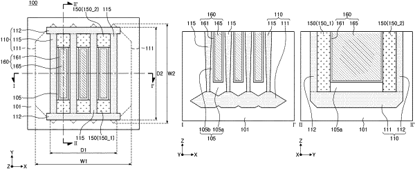
1. A semiconductor device, comprising:
a substrate;
a substrate insulating structure embedded within the substrate, said substrate insulating structure including: (i) first sidewall insulating layers disposed on the substrate, extending along a first direction and spaced apart from each other in a second direction perpendicular to the first direction, (ii) second sidewall insulating layers disposed between the first sidewall insulating layers, in contact with the first sidewall insulating layers and spaced apart from each other in the first direction, and (iii) a lower insulating layer disposed below and in contact with each of the first sidewall insulating layers and the second sidewall insulating layers;
a gate structure having a side surface and a lower surface surrounded by the substrate insulating structure, and including a gate dielectric layer and a gate electrode on the gate dielectric layer;
an active region disposed between the substrate insulating structure and the gate structure; and
a first source/drain region and a second source/drain region spaced apart from each other on the active region.
|