| CPC H01L 29/7851 (2013.01) [H01L 29/41791 (2013.01)] | 20 Claims |

|
1. A semiconductor device comprising:
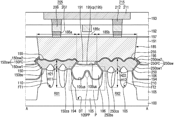
a first fin-type pattern on a substrate and extending in a first direction;
a second fin-type pattern on the substrate, wherein the second fin-type pattern is spaced apart from the first fin-type pattern in a second direction and extends in the first direction;
a first epitaxial pattern on and connected to the first fin-type pattern;
a second epitaxial pattern on and connected to the second fin-type pattern, wherein the second epitaxial pattern is spaced apart from the first epitaxial pattern;
a lower field insulating film on the substrate and extending on a sidewall of the first fin-type pattern and a sidewall of the second fin-type pattern, wherein the lower field insulating film includes a protrusion protruding in a third direction;
a lower epitaxial etch stop film extending along a top surface of the lower field insulating film, a sidewall of the first epitaxial pattern, and a sidewall of the second epitaxial pattern;
an upper field insulating film on the lower epitaxial etch stop film and extending on a portion of the sidewall of the first epitaxial pattern and a portion of the sidewall of the second epitaxial pattern;
an upper epitaxial etch stop film extending along a top surface of the upper field insulating film; and
a source/drain contact on and connected to the first epitaxial pattern and the second epitaxial pattern,
wherein the protrusion of the lower field insulating film is between the first fin-type pattern and the second fin-type pattern, and
wherein a vertical level of a top surface of the protrusion of the lower field insulating film increases and then decreases with increasing distance from the sidewall of the first fin-type pattern.
|