| CPC H01L 29/785 (2013.01) [H01L 23/5286 (2013.01); H01L 27/0886 (2013.01); H01L 29/0669 (2013.01); H01L 29/41791 (2013.01)] | 20 Claims |

|
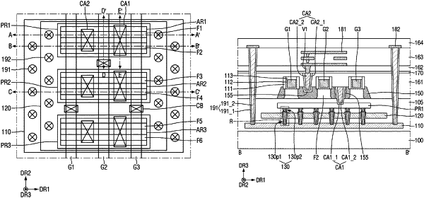
1. A semiconductor device, comprising:
a base substrate;
a first electrode plate on the base substrate;
a first power rail on the first electrode plate, the first power rail extending in a first horizontal direction and overlapping the first electrode plate in a vertical direction;
a second power rail on the first electrode plate, the second power rail extending in the first horizontal direction and overlapping the first electrode plate in the vertical direction, and the second power rail being spaced apart from the first power rail in a second horizontal direction different from the first horizontal direction;
a first power rail contact electrically connecting the first electrode plate and the first power rail;
an insulating layer on the base substrate, the insulating layer surrounding the first electrode plate, the first power rail, and the second power rail; and
a gate electrode extending in the second horizontal direction on the insulating layer.
|
|
13. A semiconductor device, comprising:
a base substrate;
a first electrode plate on the base substrate;
a second electrode plate on the first electrode plate;
a first power rail extending in a first horizontal direction on the second electrode plate;
a second power rail extending in the first horizontal direction on the second electrode plate, the second power rail being spaced apart from the first power rail in a second horizontal direction different from the first horizontal direction;
an active pattern extending in the first horizontal direction on the first power rail;
a gate electrode which extends in the second horizontal direction on the active pattern and intersects each of the first and second power rails;
a source/drain region on opposite side walls of the gate electrode;
a source/drain contact which penetrates the source/drain region in a vertical direction on a first side wall of the gate electrode, the source/drain contact electrically connecting the source/drain region to the first power rail; and
a power rail contact which penetrates the second electrode plate in the vertical direction, the power rail contact electrically connecting the first electrode plate and the first power rail.
|
|
20. A semiconductor device, comprising:
a base substrate;
a first electrode plate on the base substrate, the first electrode plate having a flat plate shape;
a second electrode plate on the first electrode plate, the second electrode plate having a flat plate shape;
a first power rail which extends in a first horizontal direction on the second electrode plate, the first power rail overlapping each of the first and second electrode plates in a vertical direction;
a second power rail which extends in the first horizontal direction on the second electrode plate, the second power rail being spaced apart from the first power rail in a second horizontal direction different from the first horizontal direction, and the second power rail overlapping each of the first and second electrode plates in the vertical direction;
a first power rail contact which penetrates the second electrode plate in the vertical direction, the first power rail contact electrically connecting the first electrode plate and the first power rail;
a second power rail contact which extends in the vertical direction on an upper surface of the second electrode plate, the second power rail contact electrically connecting the second electrode plate to the second power rail;
an insulating layer on the base substrate, the insulating layer surrounding the first electrode plate, the second electrode plate, the first power rail, and the second power rail;
a gate electrode extending in the second horizontal direction on the insulating layer;
a source/drain region on opposite side walls of the gate electrode;
a first source/drain contact which penetrates the source/drain region in the vertical direction on a first side wall of the gate electrode, the first source/drain contact electrically connecting the source/drain region to the first power rail; and
a second source/drain contact which extends from an upper surface of the source/drain region in the vertical direction, the second source/drain contact being on a second side wall of the gate electrode opposite to the first side wall of the gate electrode.
|