| CPC H01L 29/7813 (2013.01) [H01L 29/1095 (2013.01); H01L 29/407 (2013.01); H01L 29/66734 (2013.01)] | 2 Claims |
|
1. A semiconductor device comprising:
a semiconductor switching element including:
a drift layer having a first conductive type;
a body region having a second conductive type and arranged on the drift layer;
a first impurity region having the first conductive type, arranged in a surface portion of the body region in the body region and having an impurity concentration higher than the drift layer;
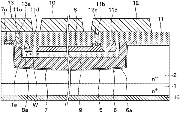
a plurality of trench gate structures, each of which includes a trench having one direction as a longitudinal direction and reaching the drift layer from the first impurity region with penetrating the body region, and each of which has a double-layered structure in which a shield electrode, an intermediate insulation film, and a gate electrode layer are stacked in order through an insulation film in the trench;
a high impurity concentration layer having the first conductivity type or the second conductive type, arranged on a side opposite to the body region to sandwich the drift layer between the high impurity concentration layer and the body region, and having an impurity concentration higher than the drift layer;
an interlayer insulation film arranged on the trench gate structures, the body region and the first impurity region, and having a contact hole connecting the body region and the first impurity region;
an upper electrode electrically connected to the first impurity region and the body region through the contact hole; and
a lower electrode electrically connected to the high impurity concentration layer;
wherein the shield electrode extends outward from an end portion of the gate electrode layer, and the intermediate insulation film is arranged between the shield electrode and a bottom surface of the gate electrode layer and between the shield electrode and the end portion of the gate electrode layer,
wherein a distance of a portion between the end portion of the gate electrode layer and the shield electrode in the one direction and having an insulation property is defined as an effective insulation distance,
wherein the effective insulation distance is larger than a thickness of a portion of the intermediate insulation film located at a bottom portion of the gate electrode layer,
wherein the interlayer insulation film further has an embedded insulation film embedded between the intermediate insulation film and the end portion of the gate electrode layer,
wherein only the intermediate insulation film and the embedded insulation film are arranged between the end portion of the gate electrode layer and the shield electrode in the one direction, and
wherein the effective insulation distance is a value equal to a sum of a thickness of a portion of the intermediate insulation film located at the end portion of the gate electrode layer and a width of the embedded insulation film.
|