| CPC H01L 29/7787 (2013.01) | 18 Claims |
|
1. A semiconductor device comprising:
a first electrode;
a second electrode, a direction from the first electrode to the second electrode being along a first direction;
a third electrode including a first electrode portion, a position of the first electrode portion in the first direction being between a position of the first electrode in the first direction and a position of the second electrode in the first direction;
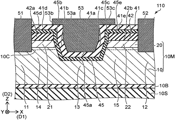
a semiconductor member including a first semiconductor region and a second semiconductor region,
the first semiconductor region including Alx1Ga1-x1N (0≤x1<1), the first semiconductor region includes a first partial region, a second partial region, a third partial region, a fourth partial region, and a fifth partial region, a direction from the first partial region to the first electrode, a direction from the second partial region to the second electrode, and a direction from the third partial region to the first electrode portion being along a second direction, the second direction crossing the first direction, a position of the fourth partial region in the first direction being between a position of the first partial region in the first direction and a position of the third partial region in the first direction, a position of the fifth partial region in the first direction being between the position of the third partial region in the first direction and a position of the second partial region in the first direction, and
the second semiconductor region including Alx2Ga1-x2N (0<x2<1, x1<x2), the second semiconductor region including a first semiconductor portion and a second semiconductor portion, a direction from the fourth partial region to the first semiconductor portion being along the second direction, a direction from the fifth partial region to the second semiconductor portion being along the second direction, the first semiconductor portion being electrically connected with the first electrode, the second semiconductor portion being electrically connected with the second electrode;
a first insulating member including a first insulating region, the first insulating region being located between the third partial region and the first electrode portion in the second direction, at least a part of the first insulating region being located between the fourth partial region and the fifth partial region in the first direction; and
a nitride member including a first nitride region, the first nitride region being located between the third partial region and the first insulating region in the second direction, the first nitride region including a plurality of first nitride portions and a plurality of second nitride portions, one of the first nitride portions being between one of the second nitride portions and an other one of the second nitride portions in a stacking direction from the semiconductor member to the first electrode portion, a composition of the one of the first nitride portions being different from a composition of the one of the second nitride portions and different from a composition of the other one of the second nitride portions,
wherein
the nitride member further comprises one or more third nitride portions,
the one or more third nitride portion is located between the one of the first nitride portions and the one of the second nitride portions in the stacking direction, and
a composition of the one or more third nitride portions is different from the composition of the one of the first nitride portions, and is different from the composition of the other one of the second nitride portions.
|