| CPC H01L 29/7397 (2013.01) [H01L 23/5228 (2013.01); H01L 29/4236 (2013.01); H01L 29/66348 (2013.01); H01L 29/7393 (2013.01); H01L 29/7395 (2013.01); H03K 17/16 (2013.01); H03K 17/60 (2013.01)] | 7 Claims |

|
1. A semiconductor device, comprising:
a semiconductor part provided with first and second surfaces, the second surface being positioned on a side opposite to the first surface;
a first electrode provided on the first surface;
a second electrode provided on the second surface;
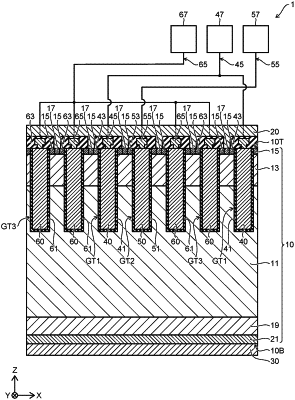
first to third control electrodes each provided at the second surface side of the semiconductor part with a trench gate structure; and
first to third control pads electrically connected to the first to third control electrodes, respectively, the first control pad being electrically connected to at least a first control electrode, the second control pad being electrically connected to at least a second control electrode, the third control pad being electrically connected to at least a third control electrode, the first to third control pads being electrically isolated from each other so that, while a prescribed voltage is applied between the first and second electrodes,
a first on-voltage and a first off-voltage are applied between the first control pad and the second electrode, the first on-voltage being applied until the first off-voltage being applied, the first on-voltage being higher than a threshold voltage of the first control electrode, the first off-voltage being lower than the threshold voltage of the first control electrode,
a second on-voltage and a second off-voltage are applied between the second control pad and the second electrode, the second on-voltage being applied until the second off-voltage being applied, the second off-voltage being applied before the first off-voltage being applied between the first control pad and the second electrode, the second on-voltage being higher than a threshold voltage of the second control electrode, the second off-voltage being lower than the threshold voltage of the second control electrode, and
a third on-voltage and a third off-voltage are applied between the third control pad and the second electrode, the third on-voltage being applied until the third off-voltage being applied, the third off-voltage being applied before the first off-voltage being applied between the first control pad and the second electrode, the third on-voltage being higher than a threshold voltage of the third control electrode, the third off-voltage being lower than the threshold voltage of the third control electrode and higher than the second off-voltage.
|