| CPC H01L 29/66984 (2013.01) [H10N 50/20 (2023.02)] | 14 Claims |
|
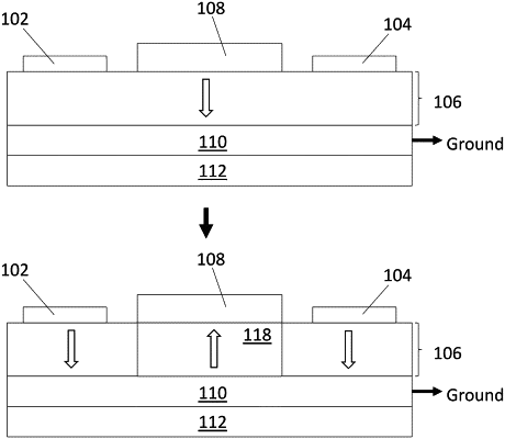
1. A voltage-controlled spin transistor comprising:
a spin injector contact;
a spin detector contact;
a layer of a multiferroic material having a first density of antiferromagnetic and ferroelectric domain boundaries that forms a three-dimensional channel for the propagation of magnons between the spin injector contact and the spin detector contact when said magnons are excited in the layer of multiferroic material by the net angular momentum of spin current injected into the multiferroic material from the spin injector contact, the layer of multiferroic material having a top surface and a bottom surface, wherein the propagation of the magnons extends into the multiferroic material below the top surface of the layer of multiferroic material and above the bottom surface of the layer of multiferroic material;
at least one top gate contact; and
at least one bottom gate contact,
wherein the at least one top gate contact and the at least one bottom gate contact are configured to apply a gate voltage across the channel, the voltage-controlled spin transistor characterized in that the application of the gate voltage across the channel increases the density of the antiferromagnetic and ferroelectric domain boundaries in the multiferroic material.
|