| CPC H01L 29/66795 (2013.01) [H01L 21/823431 (2013.01); H01L 27/0924 (2013.01)] | 15 Claims |
|
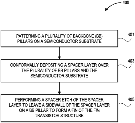
1. A method of forming a fin transistor structure, comprising:
patterning a plurality of backbone pillars on a semiconductor substrate;
conformally depositing a spacer layer over the plurality of backbone pillars and the semiconductor substrate; and
performing a spacer etch of the spacer layer to leave a first sidewall and a second sidewall of the spacer layer on a backbone pillar to form a first fin and a second fin, respectively, of the fin transistor structure, wherein the first fin has a first side higher than a second side, and the second fin has a first side higher than a second side, and wherein the first side of the first fin faces toward the first side of the second fin.
|