| CPC H01L 29/66545 (2013.01) [H01L 21/76224 (2013.01); H01L 29/0665 (2013.01); H01L 29/42392 (2013.01); H01L 29/66742 (2013.01)] | 20 Claims |
|
1. A method, comprising:
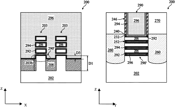
forming semiconductor fins over a substrate, wherein each semiconductor fin includes a stack of alternating SiGe layers and Si layers disposed over a protruding portion of the substrate;
forming isolation features including silicon oxide over the substrate, thereby separating bottom portions of the semiconductor fins from each other;
depositing a capping layer including SiGe over the semiconductor fins, wherein Ge in the capping layer diffuses into the isolation features to form a Ge-doped layer in the isolation features;
performing a first etching process to remove remaining portions of the capping layer and portions of the Ge-doped layer;
performing a second etching process to remove the SiGe layers and remaining portions of the Ge-doped layer, thereby forming openings between the Si layers and exposing sidewalls of the protruding portion of the substrate; and
forming a metal gate stack in the openings and over the semiconductor fins, such that the metal gate stack extends to directly contact the sidewalls of the protruding portion of the substrate.
|