US 12,080,774 B2
Semiconductor device and method of fabricating the same
Ho Kyun An, Seoul (KR); and Su Min Cho, Hwaseong-si (KR)
Assigned to SAMSUNG ELECTRONICS CO., LTD., Suwon-si (KR)
Filed by Samsung Electronics Co., Ltd., Suwon-si (KR)
Filed on Oct. 16, 2023, as Appl. No. 18/487,177.
Application 18/487,177 is a continuation of application No. 17/822,594, filed on Aug. 26, 2022, granted, now 11,824,098.
Application 17/822,594 is a continuation of application No. 17/335,455, filed on Jun. 1, 2021, granted, now 11,456,366, issued on Sep. 27, 2022.
Claims priority of application No. 10-2020-0130911 (KR), filed on Oct. 12, 2020.
Prior Publication US 2024/0038863 A1, Feb. 1, 2024
Int. Cl. H01L 29/423 (2006.01); H01L 21/02 (2006.01); H01L 27/092 (2006.01); H01L 29/161 (2006.01); H01L 29/40 (2006.01); H10B 12/00 (2023.01)
CPC H01L 29/4236 (2013.01) [H01L 21/02532 (2013.01); H01L 21/02667 (2013.01); H01L 27/092 (2013.01); H01L 29/161 (2013.01); H01L 29/401 (2013.01); H10B 12/50 (2023.02)] 20 Claims
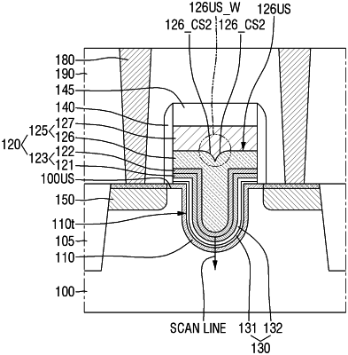
OG exemplary drawing
 
1. A semiconductor device comprising:
a substrate;
a multi-channel active pattern protruding from the substrate, and extending in a first direction;
a field insulating film disposed on the substrate, and covering a part of side walls of the multi-channel active pattern;
a silicon-germanium film on a part of side walls of the multi-channel active pattern;
a gate electrode extending in a second direction on the substrate, and covering the multi-channel active pattern; and
a gate insulating film between the silicon-germanium film and the gate electrode.