| CPC H01L 29/41791 (2013.01) [H01L 27/0886 (2013.01); H01L 29/6656 (2013.01); H01L 29/66795 (2013.01); H01L 29/7851 (2013.01)] | 20 Claims |
|
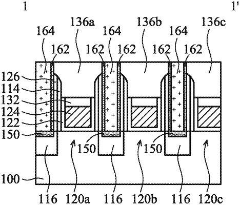
1. A semiconductor device structure, comprising:
a source/drain region formed in a semiconductor substrate;
a source/drain contact structure formed over the source/drain region;
a gate electrode layer formed over the semiconductor substrate and adjacent to the source/drain contact structure;
a first spacer and a second spacer both between the gate electrode layer and the source/drain contact structure, in isolation from one another and laterally and successively arranged from a sidewall of the gate electrode layer to a sidewall of the source/drain contact structure, wherein a sidewall of the first spacer is substantially aligned to a first side edge of the source/drain region extending in a longitudinal direction of the gate electrode layer; and
a silicide region formed in the source/drain region, wherein a top width of the silicide region is greater than a bottom width of the source/drain contact structure and less than a top width of the source/drain region.
|