| CPC H01L 29/41775 (2013.01) [H01L 29/42392 (2013.01); H01L 29/78696 (2013.01); H01L 29/7851 (2013.01); H01L 29/7853 (2013.01)] | 20 Claims |

|
1. A semiconductor device, comprising:
a first active pattern disposed on a substrate;
a device isolation layer that fills a trench which defines the first active pattern;
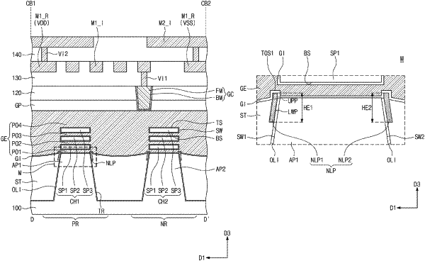
a first channel pattern and a first source/drain pattern disposed on the first active pattern, the first channel pattern including a plurality of semiconductor patterns that are stacked and spaced apart from each other;
a gate electrode that extends and runs across the first channel pattern;
a gate dielectric layer disposed between the first channel pattern and the gate electrode; and
a first passivation pattern disposed between the device isolation layer and a first sidewall of the first active pattern,
wherein the first passivation pattern includes:
an upper part that protrudes upwardly from the device isolation layer; and
a lower part that is buried in the device isolation layer,
wherein the gate dielectric layer covers the upper part of the first passivation pattern.
|