| CPC H01L 29/1054 (2013.01) [H01L 21/02057 (2013.01); H01L 21/02645 (2013.01); H01L 21/3065 (2013.01); H01L 21/308 (2013.01); H01L 21/74 (2013.01); H01L 21/823807 (2013.01); H01L 21/823821 (2013.01); H01L 21/823878 (2013.01); H01L 21/823892 (2013.01); H01L 27/0924 (2013.01); H01L 27/0928 (2013.01); H01L 29/0653 (2013.01); H01L 29/1083 (2013.01); H01L 29/66795 (2013.01); H01L 29/78 (2013.01); H01L 29/7842 (2013.01); H01L 29/7851 (2013.01); H01L 21/02532 (2013.01); H01L 21/0262 (2013.01); H01L 21/02639 (2013.01); H01L 21/02661 (2013.01)] | 20 Claims |
|
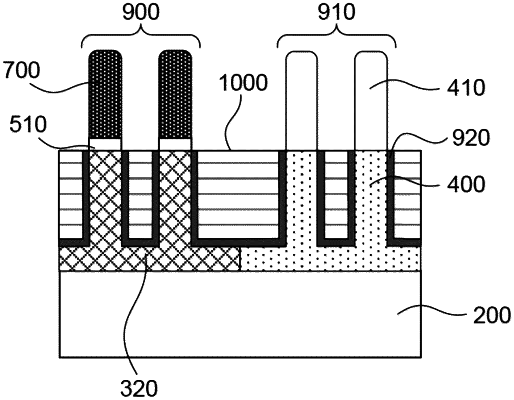
1. A structure, comprising:
a fin formed on a substrate, wherein the fin comprises:
an n-type doped region formed on a top portion of the substrate;
a silicon epitaxial layer on the n-type doped region; and
an epitaxial stack on the silicon epitaxial layer, wherein the epitaxial stack comprises:
a silicon-based seed layer in physical contact with the silicon epitaxial layer;
a first silicon germanium epitaxial sub-layer with a first germanium concentration that is substantially constant through a thickness of the first silicon germanium epitaxial sub-layer perpendicular to the substrate; and
a second silicon germanium epitaxial sub-layer with a second germanium concentration that is substantially constant through a thickness of the second silicon germanium epitaxial sub-layer perpendicular to the substrate, wherein the first germanium concentration is different from the second germanium concentration;
a liner surrounding the epitaxial stack; and
a dielectric surrounding the liner.
|