| CPC H01L 29/0665 (2013.01) [H01L 21/823468 (2013.01); H01L 29/42392 (2013.01); H01L 29/6656 (2013.01); H01L 29/66742 (2013.01); H01L 29/78618 (2013.01); H01L 29/78696 (2013.01)] | 20 Claims |
|
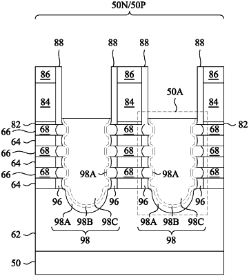
1. A method comprising:
etching a source/drain recess in a nanostructure and a fin;
growing first epitaxial layers from a sidewall of the nanostructure and a top surface of the fin in the source/drain recess;
growing a second epitaxial layer from the first epitaxial layers with a growth process, the growth process having a first bottom-up growth rate from the first epitaxial layers and having a second bottom-up growth rate from the fin and the nanostructure, the first bottom-up growth rate less than the second bottom-up growth rate; and
growing a third epitaxial layer from the second epitaxial layer.
|