| CPC H01L 27/1464 (2013.01) [H01L 27/14623 (2013.01); H01L 27/14636 (2013.01); H01L 27/14643 (2013.01); H01L 27/14685 (2013.01); H01L 27/14689 (2013.01)] | 13 Claims |

|
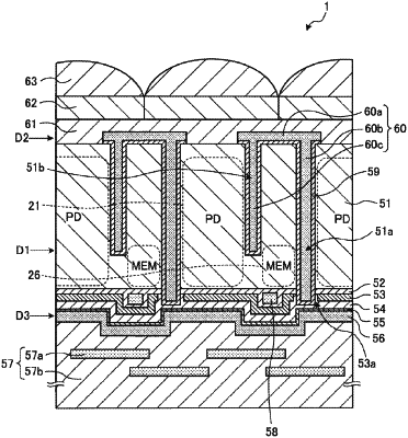
1. A solid-state imaging apparatus, comprising:
a semiconductor layer that includes:
a plurality of photoelectric conversion units configured to generate charge; and
a plurality of charge retention units configured to retain the charge generated by the plurality of photoelectric conversion units;
a trench in the semiconductor layer, wherein
the trench extends in a depth direction from a light-incident side of the semiconductor layer,
the trench is between a photoelectric conversion unit of the plurality of photoelectric conversion units and a charge retention unit of the plurality of charge retention units, and
the photoelectric conversion unit is adjacent to the charge retention unit;
a light shield wall inside the trench; and
an insulation layer provided on a side of the semiconductor layer opposite to the light-incident side, wherein
the insulation layer includes a first opening that surrounds the trench, and
a size of the first opening in the insulation layer is larger than a first area of the trench surrounded by the first opening as viewed from the light-incident side.
|