| CPC H01L 27/14636 (2013.01) [H01L 27/14623 (2013.01); H01L 27/1463 (2013.01); H01L 27/1464 (2013.01)] | 20 Claims |
|
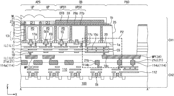
1. An image sensor comprising:
a first chip comprising a pixel region, a pad region, and an optical black region interposed between the pixel region and the pad region; and
a second chip being in contact with a first surface of the first chip and comprising circuits for driving the first chip,
wherein the first chip comprises:
a first substrate;
a device isolation portion disposed in the first substrate and defining unit pixels;
an interlayer insulating layer interposed between the first substrate and the second chip;
a connection wiring structure disposed in the interlayer insulating layer; and
a connection contact plug disposed in the interlayer insulating layer and connecting the connection wiring structure to the device isolation portion in the optical black region, and
wherein the image sensor further comprises a conductive pad disposed in the first chip or the second chip and being exposed in the pad region by a recess region penetrating the first substrate and the interlayer insulating layer, the conductive pad being electrically connected to the device isolation portion through the connection wiring structure and the connection contact plug.
|