| CPC H01L 27/14625 (2013.01) [H01L 27/14603 (2013.01); H01L 27/14621 (2013.01); H04N 23/67 (2023.01); H04N 25/11 (2023.01); H04N 25/704 (2023.01)] | 14 Claims |
|
1. An image sensor comprising:
a light sensor array comprising a plurality of light sensors configured to detect an incident light and convert the incident light into an electrical signal, the plurality of light sensors being provided in a plurality of pixels;
a spacer layer provided on the light sensor array;
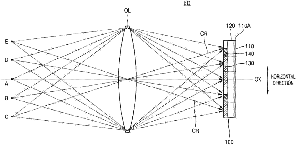
a color separation element provided on the spacer layer, and comprising a plurality of nanostructures, configured to separate the incident light into light of a plurality of colors based on a wavelength band and transmit the separated light of the plurality of colors to a corresponding one of the plurality of pixels; and
a focusing element provided on the spacer layer, and comprising a plurality of nanostructures in a region corresponding to at least one pixel among the plurality of pixels and configured to perform focusing according to an angle of the incident light,
wherein the color separation element and the focusing element are provided on a same surface of the spacer layer.
|