US 12,080,736 B2
Imaging device and electronic device
Seiichi Yoneda, Isehara (JP); Yusuke Negoro, Kaizuka (JP); Takayuki Ikeda, Atsugi (JP); and Shunpei Yamazaki, Setagaya (JP)
Assigned to Semiconductor Energy Laboratory Co., Ltd., Atsugi (JP)
Appl. No. 17/633,242
Filed by Semiconductor Energy Laboratory Co., Ltd., Atsugi (JP)
PCT Filed Aug. 7, 2020, PCT No. PCT/IB2020/057459
§ 371(c)(1), (2) Date Feb. 7, 2022,
PCT Pub. No. WO2021/033065, PCT Pub. Date Feb. 25, 2021.
Claims priority of application No. 2019-151829 (JP), filed on Aug. 22, 2019; application No. 2019-203331 (JP), filed on Nov. 8, 2019; application No. 2020-007843 (JP), filed on Jan. 21, 2020; and application No. 2020-110652 (JP), filed on Jun. 26, 2020.
Prior Publication US 2022/0359592 A1, Nov. 10, 2022
Int. Cl. H01L 27/14 (2006.01); H01L 27/146 (2006.01)
CPC H01L 27/14616 (2013.01) [H01L 27/14649 (2013.01)] 8 Claims
OG exemplary drawing
 
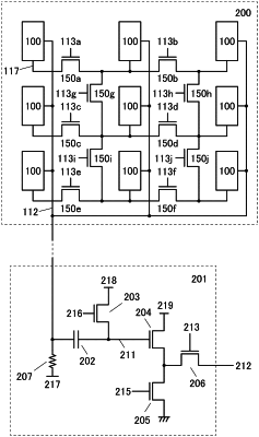
1. An imaging device comprising:
a first transistor; and
a first pixel and a second pixel each comprising a second transistor and a capacitor,
wherein one electrode of the capacitor of the first pixel and one of a source and a drain of the second transistor of the first pixel are electrically connected to one of a source and a drain of the first transistor, and
wherein one electrode of the capacitor of the second pixel and one of a source and a drain of the second transistor of the second pixel are electrically connected to the other of the source and the drain of the first transistor.