| CPC H01L 27/14612 (2013.01) [H01L 27/14643 (2013.01); H04N 25/70 (2023.01); A61B 1/05 (2013.01); B60R 11/04 (2013.01)] | 21 Claims |
|
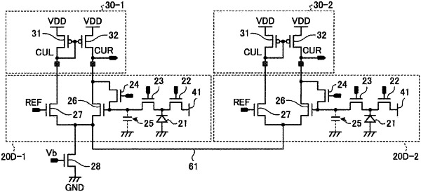
1. A solid-state imaging element comprising:
a first pixel circuit and a second pixel circuit, each including a first transistor, a second transistor and a photoelectric converter that performs photoelectric conversion on received light to generate a pixel signal, the first transistor being configured to amplify the pixel signal generated by the photoelectric converter the second transistor being configured to receive a reference signal from a reference signal generator, and
a third transistor that is shared by the first pixel circuit and the second pixel circuit, the third transistor being configured to respectively output bias current to the first transistor and the second transistor of the first and second pixel circuits.
|