| CPC H01L 27/1461 (2013.01) [H01L 27/14603 (2013.01); H01L 27/14643 (2013.01); H01L 31/107 (2013.01)] | 14 Claims |
|
1. A photodetector, comprising:
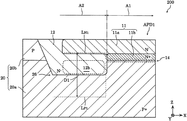
a semiconductor substrate of a first conductivity type;
a first semiconductor layer of a second conductivity type that is located above the semiconductor substrate and forms a junction with the semiconductor substrate in a first area, the second conductivity type being different from the first conductivity type; and
a second semiconductor layer of the second conductivity type that is located above the semiconductor substrate in a second area outward of the first area, the second semiconductor layer having an impurity concentration lower than an impurity concentration of the first semiconductor layer, wherein
the semiconductor substrate includes a first junction portion,
the first semiconductor layer includes a second junction portion having a higher impurity concentration than a remaining portion of the first semiconductor layer, the second junction portion being joined to the first junction portion,
the second semiconductor layer extends to a level below an interface between the first junction portion-and the second junction portion-in a thickness direction of the semiconductor substrate, and
the second semiconductor layer is in contact with both the first junction portion and the second junction portion.
|