| CPC H01L 27/1248 (2013.01) [G09G 3/32 (2013.01); H01L 25/167 (2013.01); G09G 2300/0439 (2013.01); G09G 2300/0819 (2013.01); G09G 2300/0842 (2013.01); G09G 2310/0243 (2013.01); G09G 2310/08 (2013.01); G09G 2330/04 (2013.01); G09G 2330/12 (2013.01); H01L 24/05 (2013.01); H01L 33/62 (2013.01); H01L 2224/05027 (2013.01); H01L 2224/05073 (2013.01); H01L 2224/05562 (2013.01); H01L 2224/05573 (2013.01)] | 17 Claims |

|
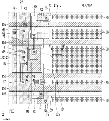
1. A light emitting display device comprising:
a pixel circuit unit having a driving transistor generating an output current;
a data distribution unit configured to apply a data voltage to the pixel circuit unit through a data line that extends in a first direction;
a plurality of signal generating units respectively configured to apply a scan signal and a light emission control signal to the pixel circuit unit through a plurality of signal lines;
a unit light emitting diode configured to receive the output current of the pixel circuit unit and attached to the pixel circuit unit;
a dummy opening formed in a region where the pixel circuit unit, the data distribution unit, and a plurality of signal generating units are not positioned; and
a signal line extending region where a plurality of signal lines extend in a second direction, the second direction crossing the first direction,
wherein the pixel circuit unit and the signal line extending region are formed to be repeated along the second direction, and
wherein the plurality of signal lines comprise a first scan line, a second scan line, a bypass control line, and a light emission signal line;
wherein the plurality of signal generating units comprise:
a first stage configured to transmit a first scan signal to the first scan line;
a second stage configured to transmit a second scan signal to the second scan line;
a third stage configured to transmit a bypass signal to the bypass control line; and
a fourth stage configured to transmit a light emission signal to the light emission signal line;
each of the first to fourth stages are positioned between two adjacent unit light emitting diodes; and
a same stage for each of the first scan signal, the second scan signal, the bypass signal, and the light emission signal is arranged along the first direction and is positioned in a left region or a right region of the light emitting display device.
|