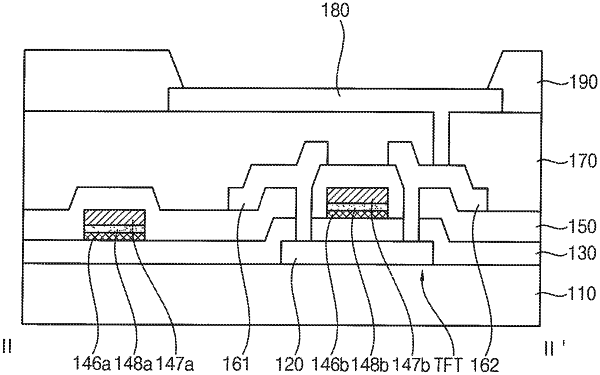
| CPC H01L 27/124 (2013.01) [H01L 27/1259 (2013.01); H10K 59/131 (2023.02); H01L 27/1218 (2013.01)] | 14 Claims |

|
1. A display substrate comprising:
a substrate;
a gate insulating layer on the substrate, the gate insulating layer comprising at least one selected from silicon oxide, silicon nitride, and silicon oxynitride; and
a wiring on the gate insulating layer,
wherein the wiring comprises a metal oxide layer comprising at least one oxide selected from tantalum (Ta), niobium (Nb), and titanium (Ti), a metal layer on the metal oxide layer and comprising copper (Cu), and an intermetallic compound layer between the metal oxide layer and the metal layer, the intermetallic compound layer comprises an intermetallic compound comprising copper, and at least one selected from tantalum, niobium, or titanium, and
a thickness of the metal oxide layer is in a range of 30 angstroms (Å) to 50 Å.
|