US 12,080,720 B2
Semiconductor device and manufacturing method thereof
Shunpei Yamazaki, Setagaya (JP); Jun Koyama, Sagamihara (JP); and Hiroyuki Miyake, Atsugi (JP)
Assigned to Semiconductor Energy Laboratory Co., Ltd., Atsugi (JP)
Filed by Semiconductor Energy Laboratory Co., Ltd., Atsugi (JP)
Filed on Jun. 8, 2023, as Appl. No. 18/207,175.
Application 18/207,175 is a continuation of application No. 17/328,171, filed on May 24, 2021, granted, now 11,776,968.
Application 17/328,171 is a continuation of application No. 16/780,034, filed on Feb. 3, 2020, granted, now 11,107,840, issued on Aug. 31, 2021.
Application 16/780,034 is a continuation of application No. 16/391,877, filed on Apr. 23, 2019, granted, now 11,107,838, issued on Aug. 31, 2021.
Application 16/391,877 is a continuation of application No. 16/277,026, filed on Feb. 15, 2019, granted, now 10,868,046, issued on Dec. 15, 2020.
Application 16/277,026 is a continuation of application No. 14/807,168, filed on Jul. 23, 2015, granted, now 10,249,647, issued on Apr. 2, 2019.
Application 14/807,168 is a continuation of application No. 14/156,845, filed on Jan. 16, 2014, granted, now 9,093,544, issued on Jul. 28, 2015.
Application 14/156,845 is a continuation of application No. 12/938,402, filed on Nov. 3, 2010, granted, now 8,633,480, issued on Jan. 21, 2014.
Claims priority of application No. 2009-255315 (JP), filed on Nov. 6, 2009.
Prior Publication US 2023/0335561 A1, Oct. 19, 2023
This patent is subject to a terminal disclaimer.
Int. Cl. H01L 27/12 (2006.01); G09G 3/20 (2006.01); G11C 19/28 (2006.01); H01L 29/04 (2006.01); H01L 29/10 (2006.01); H01L 29/24 (2006.01); H01L 29/417 (2006.01); H01L 29/423 (2006.01); H01L 29/45 (2006.01); H01L 29/786 (2006.01); H01L 29/49 (2006.01); H10K 59/121 (2023.01)
CPC H01L 27/1229 (2013.01) [G09G 3/20 (2013.01); G11C 19/28 (2013.01); H01L 27/1225 (2013.01); H01L 27/1251 (2013.01); H01L 29/045 (2013.01); H01L 29/1033 (2013.01); H01L 29/24 (2013.01); H01L 29/247 (2013.01); H01L 29/41733 (2013.01); H01L 29/42372 (2013.01); H01L 29/45 (2013.01); H01L 29/78648 (2013.01); H01L 29/7869 (2013.01); H01L 29/78693 (2013.01); G09G 2310/0267 (2013.01); G09G 2310/0275 (2013.01); G09G 2310/0286 (2013.01); H01L 27/12 (2013.01); H01L 27/1214 (2013.01); H01L 29/4908 (2013.01); H01L 29/78609 (2013.01); H10K 59/1213 (2023.02)] 8 Claims
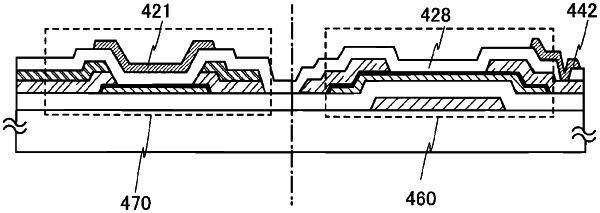
OG exemplary drawing
 
1. A display device comprising:
a pixel portion over a substrate; and
a driver circuit portion over the substrate,
wherein the pixel portion comprises a first transistor and a light-emitting element electrically connected to the first transistor,
wherein the first transistor comprises:
a first gate electrode layer over the substrate;
a first gate insulating layer over the first gate electrode layer;
a first oxide semiconductor layer in which a channel is formed over the first gate insulating layer;
a first source electrode layer comprising a region in contact with the first oxide semiconductor layer;
a first drain electrode layer comprising a region in contact with the first oxide semiconductor layer;
a second gate insulating layer over the first oxide semiconductor layer; and
a second gate electrode layer over the second gate insulating layer,
wherein the first oxide semiconductor layer comprises In, Ga, and Zn, and
wherein the first oxide semiconductor layer comprises a region which has been deposited using a target with a composition ratio of In:Ga:Zn=1:1:1.