| CPC H01L 27/1225 (2013.01) [H01L 27/1255 (2013.01); H01L 29/7869 (2013.01)] | 8 Claims |
|
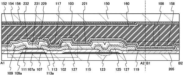
1. A display device comprising:
a gate electrode;
a first insulating film;
a first metal oxide film over the first insulating film;
a second metal oxide film over the first insulating film;
a first conductive film over the first metal oxide film;
a second conductive film over the first metal oxide film;
a second insulating film over the first metal oxide film, the second metal oxide film, the first conductive film, and the second conductive film; and
a pixel electrode over the second insulating film,
wherein the gate electrode comprises a first region overlapping with a channel formation region of the first metal oxide film,
wherein the first conductive film is electrically connected to the first metal oxide film,
wherein the second conductive film is electrically connected to the first metal oxide film,
wherein the pixel electrode is electrically connected to the first conductive film,
wherein the second metal oxide film comprises a second region,
wherein a conductivity of the second region is higher than a conductivity of the channel formation region of the first metal oxide film,
wherein the second insulating film comprises an opening,
wherein in the opening, a third insulating film is over the second metal oxide film,
wherein in the opening, the pixel electrode comprises a third region overlapping with the second metal oxide film with the third insulating film interposed therebetween,
wherein the second metal oxide film comprises a fourth region overlapping with the opening, and
wherein an entire under surface of the fourth region of the second metal oxide film is in contact with an insulating surface.
|