| CPC H01L 27/1203 (2013.01) [H01L 27/1207 (2013.01); H01L 29/66477 (2013.01); H01L 29/66628 (2013.01); H01L 29/66651 (2013.01); H01L 29/7834 (2013.01); H01L 21/823418 (2013.01); H01L 21/823814 (2013.01); H01L 29/41783 (2013.01)] | 12 Claims |
|
1. A method of manufacturing a semiconductor device, comprising steps of:
(a) providing a semiconductor substrate having:
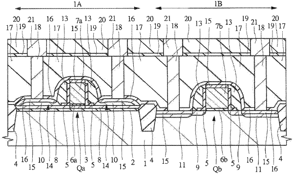
a first region including a BOX (Buried Oxide) film formed on the semiconductor substrate, an SOI (Silicon On Insulator) layer formed on the first insulating film, a first gate insulating film formed on the SOI layer, a first gate electrode formed on the first gate insulating film, and a first hard mask formed on the first gate electrode, and
a second region including a second gate insulating film formed on the semiconductor substrate, a second gate electrode formed on the second gate insulating film, and a second hard mask formed on the second gate electrode;
(b) after the step of (a), forming a first insulating film so as to cover the SOI layer, a side surface of the first gate electrode, the first hard mask, the semiconductor substrate in the second region, a side surface of the second gate electrode and the second hard mask;
(c) after the step of (b), forming a second insulating film on the side surface of the first gate electrode via the first insulating film, and forming a third insulating film on the side surface of the second gate electrode via the first insulating film, a material of each of the second insulating film and the third insulating film being different from a material of the first insulating film, the material of the second insulating film being the same as the material of the third insulating film;
(d) after the step of (c), covering the third insulating film and the first insulating film, which is exposed from the third insulating film, in the second region with a resist film;
(e) after the step of (d), performing an etching process in a state that the third insulating film and the first insulating film, which is exposed from the third insulating film, in the second region is covered with the resist film, thereby removing a portion, which is exposed from the second insulating film, of the first insulating film in the first region;
(f) after the step of (e), forming an epitaxial layer on the SOI layer exposed from the first insulating film by performing the step of (e);
(g) after the step of (f), removing a portion, which is exposed from the third insulating film, of the first insulating film in the second region in a state that a portion of the first insulating film located between the first gate electrode and the second insulating film is exposed;
(h) after the step of (g), removing the second insulating film;
(i) after the step of (h), implanting a first impurity into the SOI layer, thereby forming a first extension region in the SOI layer; and
(j) after the step of (i), forming a fourth insulating film on the side surface of the first gate electrode via the first insulating film such that the fourth insulating film is in contact with a portion, which is exposed from the first insulating film in the first region, of the side surface of the first gate electrode, a material of the fourth insulating film being the same as the material of the second insulating film.
|