| CPC H01L 27/0886 (2013.01) [H01L 29/0673 (2013.01); H01L 29/1037 (2013.01); H01L 29/42392 (2013.01); H01L 29/4966 (2013.01); H01L 21/02532 (2013.01); H01L 21/28088 (2013.01); H01L 21/30604 (2013.01); H01L 21/32139 (2013.01); H01L 21/76224 (2013.01); H01L 21/823412 (2013.01); H01L 21/823418 (2013.01); H01L 21/823431 (2013.01); H01L 21/82345 (2013.01); H01L 21/823468 (2013.01); H01L 21/823481 (2013.01); H01L 29/0847 (2013.01); H01L 29/165 (2013.01); H01L 29/66545 (2013.01); H01L 29/66636 (2013.01); H01L 29/7848 (2013.01)] | 20 Claims |

|
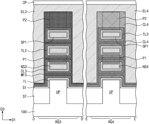
1. A semiconductor device, comprising:
a plurality of semiconductor patterns that are sequentially stacked and spaced apart from each other on a substrate;
a gate electrode on the plurality of semiconductor patterns; and
support dielectric patterns between adjacent semiconductor patterns of the plurality of semiconductor patterns, the support dielectric patterns adjacent to and not vertically overlapping the gate electrode, outer sidewalls of the plurality of semiconductor patterns are coplanar with outer sidewalls of the support dielectric patterns, the outer sidewalls of plurality of semiconductor patterns and the outer sidewalls of the support dielectric patterns are spaced apart from the gate electrode,
the gate electrode including a capping pattern and a work function pattern that are sequentially stacked on the plurality of semiconductor patterns,
the capping pattern including a first metal nitride layer including a first metal element, and a second metal nitride layer including a second metal element whose work function is greater than a work function of the first metal element,
the first metal nitride layer being disposed between the second metal nitride layer and the plurality of semiconductor patterns, and
the first metal nitride layer being thinner than the second metal nitride layer
wherein the second metal nitride layer is a different layer from the work function pattern.
|