| CPC H01L 25/18 (2013.01) [H01L 24/05 (2013.01); H01L 24/08 (2013.01); H01L 24/29 (2013.01); H01L 24/32 (2013.01); H10B 43/10 (2023.02); H10B 43/27 (2023.02); H01L 2224/0557 (2013.01); H01L 2224/08145 (2013.01); H01L 2224/29186 (2013.01); H01L 2224/32145 (2013.01); H01L 2924/1431 (2013.01); H01L 2924/14511 (2013.01)] | 8 Claims |

|
1. A semiconductor device comprising:
an insulating structure;
a plurality of horizontal layers vertically stacked and spaced apart from each other in the insulating structure, each of the plurality of horizontal layers comprising a conductive material;
a conductive material pattern on the insulating structure; and
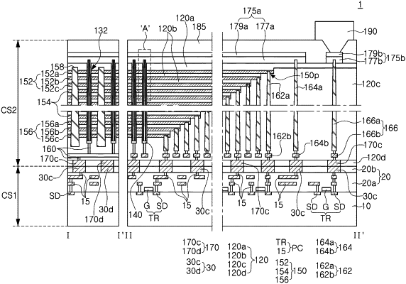
a vertical structure comprising a vertical portion penetrating through the plurality of horizontal layers, and a protruding portion extending from the vertical portion into the conductive material pattern in the insulating structure, wherein a width of the vertical portion is greater than a width of the protruding portion, and a side surface of the protruding portion is in contact with the conductive material pattern.
|