| CPC H01L 25/18 (2013.01) [H01L 23/528 (2013.01); H01L 24/03 (2013.01); H01L 24/08 (2013.01); H01L 24/09 (2013.01); H01L 24/27 (2013.01); H01L 24/32 (2013.01); H01L 24/33 (2013.01); H01L 24/83 (2013.01); H01L 25/0657 (2013.01); H01L 25/50 (2013.01); H10B 41/27 (2023.02); H10B 41/40 (2023.02); H10B 43/27 (2023.02); H10B 43/40 (2023.02); H01L 2224/08112 (2013.01); H01L 2224/08146 (2013.01); H01L 2224/09181 (2013.01); H01L 2224/32147 (2013.01); H01L 2224/33181 (2013.01); H01L 2224/80895 (2013.01); H01L 2224/80896 (2013.01); H01L 2224/83895 (2013.01); H01L 2224/83896 (2013.01); H01L 2225/06541 (2013.01); H01L 2225/06565 (2013.01); H01L 2924/14511 (2013.01)] | 20 Claims |

|
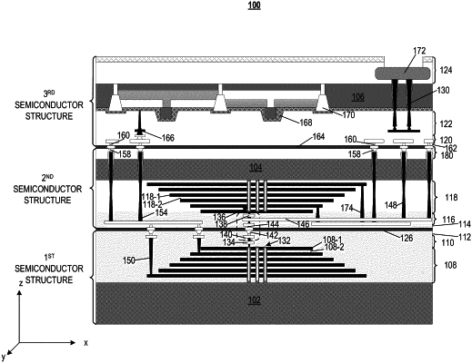
1. A method for forming a three-dimensional (3D) memory device, comprising:
forming, on a first substrate, a plurality of first NAND memory strings, a plurality of first bit lines (BLs) conductively connected to the first NAND memory strings, a plurality of first conductor layers, and a first bonding layer comprising a plurality of first bit line bonding contacts conductively connected to the first BLs, and a plurality of first word line bonding contacts conductively connected to the first conductive layers, to form a first semiconductor structure;
forming, on a second substrate, a plurality of second NAND memory strings, a plurality of second BLs conductively connected to the second NAND memory strings, a plurality of second conductor layers, and a second bonding layer comprising a plurality of second bit line bonding contacts conductively connected to the second BLs, and a plurality of second word line bonding contacts conductively connected to the second conductor layers, to form a second semiconductor structure;
bonding the first semiconductor structure and the second semiconductor structure in a face-to-face manner, such that (i) the first semiconductor structure is bonded to the second semiconductor structure, and (ii) the first BLs are respectively conductively connected to the second BLs through the bonded first and the second bit line bonding contacts at a bonding interface;
thinning the second substrate to form a semiconductor layer;
bonding a third semiconductor structure to the semiconductor layer;
thinning a third substrate of the third semiconductor structure to form another semiconductor layer; and
forming a pad-out interconnect layer above the another semiconductor layer.
|