| CPC H01L 25/0753 (2013.01) [H01L 33/38 (2013.01); H01L 33/54 (2013.01); H01L 33/62 (2013.01)] | 20 Claims |
|
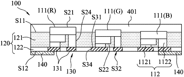
1. A light-emitting diode (LED) packaging module, comprising:
a plurality of LED chips that are spaced apart from one another, each of said LED chips including:
a chip first surface as a light-exiting surface,
a chip second surface opposite to said chip first surface,
a chip side surface that connects said chip first surface and said chip second surface, and
an electrode unit formed on said chip second surface;
a wiring layer that is disposed on said chip second surfaces of said LED chips, and that has a first wiring layer surface adjacent to said LED chips, a second wiring layer surface opposite to said first wiring layer surface, and a side wiring layer surface that is connected between said first wiring layer surface and said second wiring layer surface, said wiring layer being divided into a plurality of wiring parts that are spaced apart from each other, said first wiring layer surface contacting and being electrically connected to said electrode units of said LED chips; and
an encapsulant component including a first encapsulating layer that covers said chip side surface of each of said LED chips, and a second encapsulating layer that covers said side wiring layer surface of said wiring layer and that fills gaps among said wiring parts,
wherein
each of said LED chips has a thickness TA, said first encapsulating layer has a thickness TB, and TA and TB satisfy a relationship: TB/TA≥1.
|