| CPC H01L 24/73 (2013.01) [H01L 23/3157 (2013.01); H01L 23/481 (2013.01); H01L 23/49822 (2013.01); H01L 24/06 (2013.01); H01L 25/0652 (2013.01); H01L 2224/06177 (2013.01); H01L 2224/73204 (2013.01); H01L 2225/06513 (2013.01); H01L 2225/06517 (2013.01); H01L 2225/06541 (2013.01); H01L 2225/06589 (2013.01)] | 18 Claims |

|
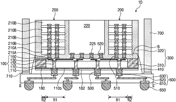
1. A semiconductor package, comprising:
a first semiconductor chip including a mount region and an overhang region;
a substrate disposed on a bottom surface at the mount region of the first semiconductor chip;
a passivation pattern disposed on a bottom surface of the substrate; and
a molding layer disposed on the substrate,
wherein the molding layer includes:
a first molding pattern disposed on a bottom surface at the overhang region of the first semiconductor chip and at least partially covering a sidewall of the substrate; and
a second molding pattern disposed directly on the first molding pattern and at least partially covering a sidewall of the first semiconductor chip, and
wherein the passivation pattern extends onto a bottom surface of the first molding pattern.
|