| CPC H01L 24/32 (2013.01) [H01L 21/321 (2013.01); H01L 21/565 (2013.01); H01L 23/3142 (2013.01); H01L 23/49562 (2013.01); H01L 23/49568 (2013.01); H01L 23/49575 (2013.01); H01L 24/83 (2013.01); H01L 2224/26145 (2013.01); H01L 2224/32245 (2013.01); H01L 2224/83815 (2013.01); H01L 2924/182 (2013.01); H01L 2924/18301 (2013.01); H01L 2924/351 (2013.01)] | 8 Claims |
|
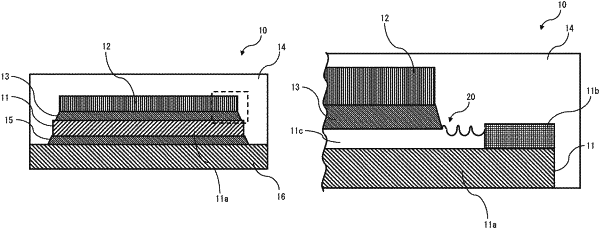
8. A semiconductor device comprising:
a semiconductor element including a body portion formed in a plate shape, a single layer of protection film provided along an outer periphery on one surface of the semiconductor body portion, and a metal thin film formed directly on said one surface of the semiconductor body portion and provided adjacently to and contacting an inner edge of the single layer of protection film on the one surface of the semiconductor body portion;
a metal member joined to a surface of the metal thin film, by solder; wherein
the surface of an outer periphery of the metal thin film, on its surface facing away from said body portion, includes a projection portion projecting from the surface of the metal thin film, such that the projection portion stands between that part of the metal thin film on the inner side from the protection portion, and said single layer of protection film, and thereby forms a barrier between the solder and the single layer of protection film, such that the solder is prevented from coming into contact with both of the metal thin film and the single layer of protection film at any one point.
|