| CPC H01L 24/29 (2013.01) [B23K 1/0016 (2013.01); B32B 15/01 (2013.01); H01L 24/32 (2013.01); B23K 2101/40 (2018.08); B23K 2103/12 (2018.08); B23K 2103/166 (2018.08); H01L 2224/29083 (2013.01); H01L 2224/29111 (2013.01); H01L 2224/29147 (2013.01); H01L 2224/29155 (2013.01); H01L 2224/2918 (2013.01); H01L 2224/29184 (2013.01); H01L 2224/32225 (2013.01)] | 18 Claims |
|
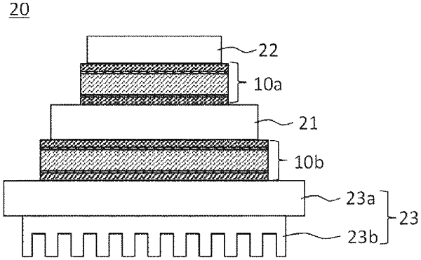
1. A layered bonding material comprising:
a base material;
a first solder section stacked on a first surface of the base material; and
a second solder section stacked on a second surface of the base material, wherein
a coefficient of linear expansion of the base material is 5.5 to 15.5 ppm/K,
the first solder section and the second solder section are made of lead-free solder, and
both of a thickness of the first solder section and a thickness of the second solder section are 0.05 to 1.0 mm.
|