| CPC H01L 24/20 (2013.01) [H01L 23/49811 (2013.01); H01L 23/49833 (2013.01); H01L 24/19 (2013.01); H01L 23/3121 (2013.01); H01L 23/3135 (2013.01); H01L 24/04 (2013.01); H01L 24/06 (2013.01); H01L 2224/04042 (2013.01); H01L 2224/06181 (2013.01); H01L 2224/214 (2013.01); H01L 2224/215 (2013.01); H01L 2924/01029 (2013.01); H01L 2924/13055 (2013.01); H01L 2924/13091 (2013.01); H01L 2924/15153 (2013.01)] | 20 Claims |

|
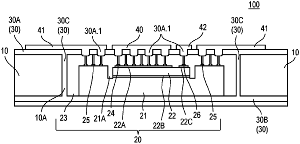
1. A semiconductor device module, comprising:
a package carrier comprising an opening, wherein in the opening there is disposed a semiconductor package comprising:
a semiconductor die, an encapsulant, and first vertical contacts, wherein the encapsulant at least partially covers the semiconductor die, and the first vertical contacts are connected to the semiconductor die;
a first outer metallic contact layer electrically connected to the first vertical contacts; and
a laminate layer covering at least partially the package carrier and the semiconductor die,
wherein the laminate layer forms a contiguous ring that surrounds the opening of the package carrier.
|