| CPC H01L 24/08 (2013.01) [H01L 24/80 (2013.01); H01L 25/0657 (2013.01); H01L 25/18 (2013.01); H01L 25/50 (2013.01); H01L 2224/08145 (2013.01); H01L 2224/80895 (2013.01); H01L 2224/80896 (2013.01); H01L 2924/1431 (2013.01); H01L 2924/1436 (2013.01)] | 20 Claims |
|
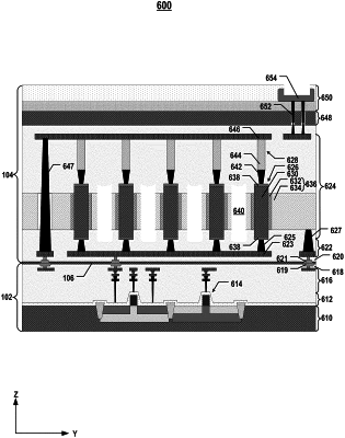
1. A three-dimensional (3D) memory device, comprising:
a first semiconductor structure comprising a peripheral circuit;
a second semiconductor structure comprising:
an array of memory cells, each of the memory cells comprising a vertical transistor extending in a first direction, and a storage unit coupled to the vertical transistor; and
a plurality of bit lines coupled to the memory cells and each extending in a second direction perpendicular to the first direction,
wherein the vertical transistor comprises a semiconductor body extending in the first direction, and a gate structure in contact with two opposite sides of the semiconductor body in the second direction; and
a respective one of the bit lines and a respective storage unit are coupled to opposite ends of each one of the memory cells in the first direction; and
a bonding interface between the first semiconductor structure and the second semiconductor structure in the first direction, wherein the array of memory cells is coupled to the peripheral circuit across the bonding interface.
|