| CPC H01L 24/05 (2013.01) [H01L 24/02 (2013.01); H01L 24/04 (2013.01); H01L 24/29 (2013.01); H01L 24/32 (2013.01); H01L 24/33 (2013.01); H01L 24/83 (2013.01); H10K 59/131 (2023.02); H01L 2224/02181 (2013.01); H01L 2224/02185 (2013.01); H01L 2224/04026 (2013.01); H01L 2224/05073 (2013.01); H01L 2224/05124 (2013.01); H01L 2224/05139 (2013.01); H01L 2224/05147 (2013.01); H01L 2224/05166 (2013.01); H01L 2224/0518 (2013.01); H01L 2224/05551 (2013.01); H01L 2224/05553 (2013.01); H01L 2224/05564 (2013.01); H01L 2224/05573 (2013.01); H01L 2224/05686 (2013.01); H01L 2224/0569 (2013.01); H01L 2224/05693 (2013.01); H01L 2224/29499 (2013.01); H01L 2224/32227 (2013.01); H01L 2224/32238 (2013.01); H01L 2224/331 (2013.01); H01L 2224/83048 (2013.01); H01L 2224/83191 (2013.01); H01L 2224/83192 (2013.01); H01L 2224/83201 (2013.01); H01L 2224/8322 (2013.01); H01L 2224/83951 (2013.01)] | 13 Claims |

|
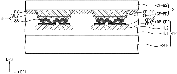
1. A display device comprising:
a substrate;
a driving pad disposed on the substrate;
an insulating layer exposing the driving pad and disposed on the substrate;
a circuit board including a circuit pad overlapping the driving pad; and
a connector disposed between the circuit board and the insulating layer and comprising a plurality of conductive particles electrically connecting the driving pad and the circuit pad,
wherein the driving pad comprising:
a first pad disposed on the substrate; and
a second pad disposed on the first pad and having a thickness with plurality of openings therein extending through the thickness of the second pad, said plurality of openings exposing the first pad, and
wherein the insulating layer covers at least part of the second pad without covering the plurality of openings.
|