| CPC H01L 23/552 (2013.01) [H01L 21/4853 (2013.01); H01L 21/4857 (2013.01); H01L 21/78 (2013.01); H01L 23/3114 (2013.01); H01L 23/49816 (2013.01); H01L 23/49822 (2013.01); H01L 23/49838 (2013.01)] | 22 Claims |

|
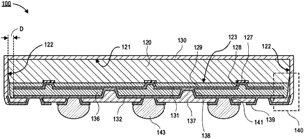
1. An electronic package, comprising:
a die having a first surface, a second surface opposite the first surface, and sidewall surfaces;
a redistribution layer over the first surface of the die, wherein the redistribution layer comprises a first conductive layer, wherein the redistribution layer comprises a first dielectric layer that separates the first conductive layer from the first surface of the die, and a second dielectric layer that separates the first conductive layer from a second conductive layer;
an under ball metallization (UBM) layer over the redistribution layer;
a conductive shield over the sidewall surfaces of the die and the second surface of the die, wherein the conductive shield is in direct contact with the UBM layer, and wherein the conductive shield horizontally overlaps the UBM layer; and
a plurality of balls in direct contact with the UBM layer on a side of the UBM layer opposite the die, wherein the conductive shield is laterally spaced apart from the solder balls.
|