| CPC H01L 23/5387 (2013.01) [H01L 23/49866 (2013.01); H01L 23/5386 (2013.01); H01L 24/16 (2013.01); H01L 25/16 (2013.01); H01L 25/18 (2013.01); H01L 2224/16227 (2013.01)] | 20 Claims |
|
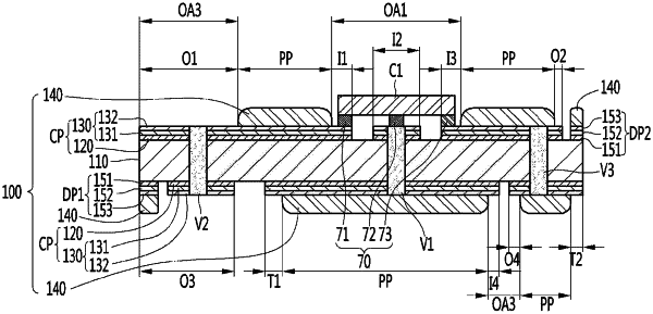
1. A flexible circuit board comprising:
a substrate;
a first conductive pattern part disposed under a first surface of the substrate;
a second conductive pattern part and a first dummy pattern part disposed over a second surface opposite to the first surface of the substrate;
a first protection layer disposed under the first conductive pattern part; and
a second protection layer disposed over the second conductive pattern part and the first dummy pattern part,
wherein the first dummy pattern part is vertically overlapped with the first conductive pattern part disposed at an outermost periphery of the substrate, the first protective layer and the second protective layer, and
wherein the first conductive pattern part includes:
a first wiring pattern layer, and
a first plating layer disposed under the first wiring pattern layer and including tin (Sn);
wherein the first dummy pattern part includes:
a second wiring pattern layer, and
a second plating layer disposed over the second wiring pattern layer and including tin (Sn),
wherein a thickness of the second plating layer of the first dummy pattern part under the second protective layer is different from a thickness of the first plating layer of the first conductive pattern part over the first protective layer.
|