| CPC H01L 23/5283 (2013.01) [H01L 23/5226 (2013.01); H10B 43/27 (2023.02); H10B 43/40 (2023.02)] | 20 Claims |
|
1. A semiconductor device comprising:
a lower horizontal pattern;
a stacked structure disposed on the lower horizontal pattern, the stacked structure including a plurality of insulation layers and a plurality of gate electrode layers;
a plurality of channel structures extending through the stacked structure;
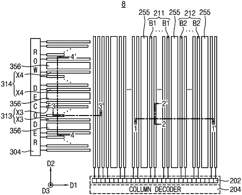
a first bit line group including a plurality of first bit lines disposed on the stacked structure, the plurality of first bit lines is arranged in a first direction and extends in a second direction intersecting with the first direction, and each of the plurality of first bit lines is electrically connected to corresponding one of the plurality of channel structures;
a second bit line group including a plurality of second bit lines disposed on the stacked structure, the plurality of second bit lines is arranged in the first direction and extends in the second direction, and each of the plurality of second bit lines is electrically connected to corresponding one of the plurality of channel structures;
a first line identifier disposed between the first bit line group and the second bit line group, the first line identifier is adjacent to a first bit line of the plurality of first bit lines and a second bit line of the plurality of second bit lines; and
at least one contact plug disposed between the first line identifier and the lower horizontal pattern,
wherein the plurality of insulation layers and the plurality of gate electrode layers are alternately stacked in a third direction intersecting with the first direction and the second direction, and
wherein each of the plurality of channel structures extends in the third direction,
wherein the first line identifier is at the same level as the plurality of first bit lines and the plurality of second bit lines,
wherein a first distance between the first bit line group and the second bit line group is greater than a second distance between first bit lines adjacent to each other among the plurality of first bit lines,
wherein at least one gate electrode layer of the plurality of gate electrode layers vertically overlaps with the plurality of first bit lines, the first line identifier, and the plurality of second bit lines, and
wherein the at least one contact plug is configured to connect the first line identifier to the lower horizontal pattern.
|