| CPC H01L 23/5283 (2013.01) [H01L 21/76816 (2013.01); H01L 21/76829 (2013.01); H01L 23/5223 (2013.01); H01L 23/5226 (2013.01)] | 13 Claims |

|
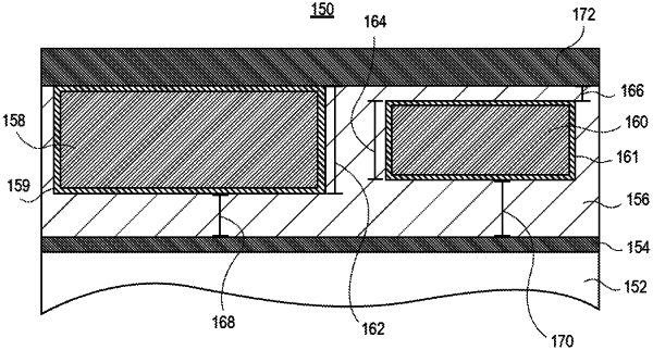
1. An integrated circuit structure, comprising:
an inter-layer dielectric (ILD) layer above a substrate; and
a plurality of conductive interconnect lines in the ILD layer, the plurality of conductive interconnect lines comprising:
a first conductive interconnect line; and
a second conductive interconnect line immediately adjacent to the first conductive interconnect line, the second conductive interconnect line having a bottommost surface above a bottommost surface of the first conductive interconnect line, and the second conductive interconnect line having an uppermost surface below an uppermost surface of the first conductive interconnect line, wherein the ILD layer is on the uppermost surface of the second conductive interconnect line,
wherein the second conductive interconnect line has a width less than a width of the first conductive interconnect line.
|
|
7. A computing device, comprising:
a board; and
a component coupled to the board, the component including an integrated circuit structure, comprising:
an inter-layer dielectric (ILD) layer above a substrate; and
a plurality of conductive interconnect lines in the ILD layer, the plurality of conductive interconnect lines comprising:
a first conductive interconnect line; and
a second conductive interconnect line immediately adjacent to the first conductive interconnect line, the second conductive interconnect line having a bottommost surface above a bottommost surface of the first conductive interconnect line, and the second conductive interconnect line having an uppermost surface below an uppermost surface of the first conductive interconnect line, wherein the ILD layer is on the uppermost surface of the second interconnect line,
wherein the second conductive interconnect line has a width less than a width of the first conductive interconnect line.
|