| CPC H01L 23/49838 (2013.01) [H01L 21/6835 (2013.01); H01L 23/49816 (2013.01); H01L 23/49894 (2013.01); H01L 21/563 (2013.01); H01L 21/565 (2013.01); H01L 23/3107 (2013.01); H01L 23/3128 (2013.01); H01L 23/3171 (2013.01); H01L 24/09 (2013.01); H01L 24/13 (2013.01); H01L 24/17 (2013.01); H01L 2221/68345 (2013.01); H01L 2221/68359 (2013.01); H01L 2224/13082 (2013.01); H01L 2224/13111 (2013.01); H01L 2224/13147 (2013.01); H01L 2224/17505 (2013.01); H01L 2924/3511 (2013.01)] | 20 Claims |
|
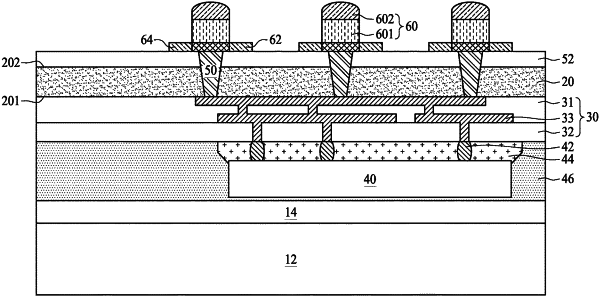
1. A method for manufacturing a semiconductor device, comprising:
depositing a dielectric layer over a first carrier substrate;
forming a first interconnection layer over a first surface of the dielectric layer;
disposing an electronic component over the first interconnection layer;
bonding the electronic component to a second carrier substrate and releasing the first carrier substrate from the dielectric layer;
forming a plurality of conductive structures through the dielectric layer and electrically connected to the first interconnection layer subsequent to depositing the dielectric layer over the first carrier substrate, wherein each of the conductive structures has a tapered profile; and
forming a plurality of electrical conductors over a second surface of the dielectric layer and electrically connected to the plurality of conductive structures.
|