| CPC H01L 23/49827 (2013.01) [H01L 23/481 (2013.01); H01L 23/49894 (2013.01); H01L 25/065 (2013.01); H01L 25/18 (2013.01); H05K 1/115 (2013.01); H05K 3/28 (2013.01); H05K 3/445 (2013.01); H01L 23/13 (2013.01); H01L 23/15 (2013.01); H01L 24/13 (2013.01); H01L 24/16 (2013.01); H01L 24/29 (2013.01); H01L 24/32 (2013.01); H01L 24/48 (2013.01); H01L 24/73 (2013.01); H01L 2224/0401 (2013.01); H01L 2224/04042 (2013.01); H01L 2224/13109 (2013.01); H01L 2224/13144 (2013.01); H01L 2224/13147 (2013.01); H01L 2224/16145 (2013.01); H01L 2224/16146 (2013.01); H01L 2224/16165 (2013.01); H01L 2224/16227 (2013.01); H01L 2224/2919 (2013.01); H01L 2224/32225 (2013.01); H01L 2224/48091 (2013.01); H01L 2224/48227 (2013.01); H01L 2224/73257 (2013.01); H01L 2224/81805 (2013.01); H01L 2224/8385 (2013.01); H01L 2225/0651 (2013.01); H01L 2225/06517 (2013.01); H01L 2225/06572 (2013.01); H01L 2924/14 (2013.01); H01L 2924/1432 (2013.01); H01L 2924/1434 (2013.01); H01L 2924/1461 (2013.01); H01L 2924/15787 (2013.01); H01L 2924/15788 (2013.01); H01L 2924/1579 (2013.01); H01L 2924/381 (2013.01); H05K 2201/09154 (2013.01); H05K 2201/09563 (2013.01); H05K 2201/09581 (2013.01); H05K 2201/0959 (2013.01); H05K 2201/09854 (2013.01); H05K 2203/0594 (2013.01)] | 20 Claims |
|
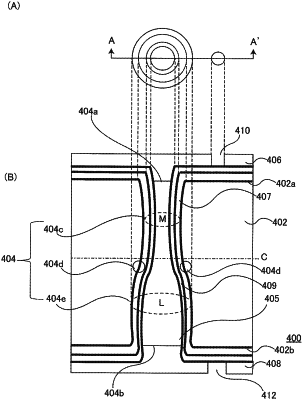
1. A through-hole electrode substrate comprising:
a substrate including a through-hole extending from a first aperture of a first surface to a second aperture of a second surface, an area of the second aperture being larger than an area of the first aperture, the through-hole having a minimum aperture part between the first aperture and the second aperture, an area of the minimum aperture part being the smallest among a plurality of areas of the through-hole in a planar view;
a first member arranged within the through-hole; and
an insulating resin layer contacting the first member exposed to one of the first surface and the second surface.
|