| CPC H01L 23/49816 (2013.01) [H01L 23/49822 (2013.01); H01L 24/03 (2013.01); H01L 24/05 (2013.01); H01L 24/16 (2013.01); H01L 27/14618 (2013.01); H01L 2224/0219 (2013.01); H01L 2224/03019 (2013.01); H01L 2224/0347 (2013.01); H01L 2224/0401 (2013.01); H01L 2224/05647 (2013.01); H01L 2224/16225 (2013.01)] | 14 Claims |
|
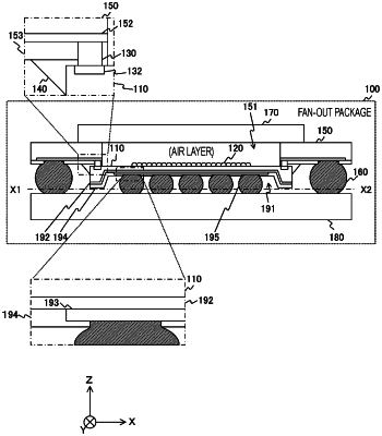
1. A semiconductor package, comprising:
a semiconductor substrate and a pad provided on one surface of the semiconductor substrate;
an insulating layer configured to cover a different surface of the semiconductor substrate;
a metal layer configured to cover the insulating layer;
an interposer substrate on which a wire, configured to connect to the pad, is formed;
a signal transmission solder ball configured to join the wire and a predetermined mounting substrate to transmit a predetermined electrical signal; and
a solder member configured to join the metal layer and the predetermined mounting substrate.
|