| CPC H01L 23/4951 (2013.01) [H01L 23/145 (2013.01); H10B 12/50 (2023.02)] | 13 Claims |

|
1. An apparatus comprising:
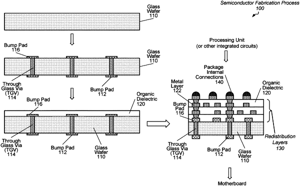
a first glass package substrate comprising:
redistribution layers between a first integrated circuit and a first side of a first glass wafer; and
bump pads directly placed on:
pads of a motherboard; and
a second side different than the first side of the first glass wafer; and
wherein responsive to a potential being applied to a first node of one of the first integrated circuit and a first component on the motherboard, a current is conveyed from the first node to a second node through the first glass package substrate.
|