| CPC H01L 23/3135 (2013.01) [H01L 21/563 (2013.01); H01L 23/3128 (2013.01); H01L 23/49816 (2013.01); H01L 24/16 (2013.01); H01L 25/0657 (2013.01); H01L 2224/16225 (2013.01); H01L 2225/0651 (2013.01); H01L 2225/0652 (2013.01)] | 20 Claims |
|
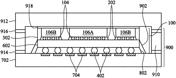
1. A method of manufacturing a semiconductor package, comprising:
attaching a first die stack to an interposer;
encapsulating the first die stack with a molding compound;
planarizing the molding compound with a backside surface of the first die stack opposite the interposer, wherein the backside surface of the first die stack is disposed a first distance from the interposer;
attaching the interposer to a substrate;
depositing a first underfill between the interposer and the substrate;
depositing a second underfill surrounding the first underfill, the second underfill being different than the first underfill;
adhering a ring to the substrate, wherein a first surface of the ring opposite the substrate is disposed at a second distance from the substrate, the second distance being less than the first distance;
adhering a lid to the backside surface of the first die stack with a thermal interface material (TIM), wherein the TIM is disposed between the molding compound and the lid, wherein a first projection area of the TIM on the substrate is greater than a second projection area of the first die stack on the substrate; and
adhering the lid to the first surface of the ring, wherein the ring and the lid encompass the first die stack, the molding compound and the TIM.
|